|
Motore di ricerca datesheet componenti elettronici |
|
|
Motore di ricerca datesheet componenti elettronici |
|
WM8281ECS/R Scheda tecnica(PDF) 14 Page - Cirrus Logic |
|
|
|||||||||||||||||||||||||||||
WM8281ECS/R Scheda tecnica(HTML) 14 Page - Cirrus Logic |
|
|
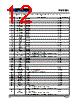
14 / 392 page  WM8281 14 Rev 4.0 ABSOLUTE MAXIMUM RATINGS Absolute Maximum Ratings are stress ratings only. Permanent damage to the device may be caused by continuously operating at or beyond these limits. Device functional operating limits and guaranteed performance specifications are given under Electrical Characteristics at the test conditions specified. ESD Sensitive Device. This device is manufactured on a CMOS process. It is therefore generically susceptible to damage from excessive static voltages. Proper ESD precautions must be taken during handling and storage of this device. Cirrus Logic tests its package types according to IPC/JEDEC J-STD-020 for Moisture Sensitivity to determine acceptable storage conditions prior to surface mount assembly. These levels are: MSL1 = unlimited floor life at <30 C / 85% Relative Humidity. Not normally stored in moisture barrier bag. MSL2 = out of bag storage for 1 year at <30 C / 60% Relative Humidity. Supplied in moisture barrier bag. MSL3 = out of bag storage for 168 hours at <30 C / 60% Relative Humidity. Supplied in moisture barrier bag. The Moisture Sensitivity Level for each package type is specified in Ordering Information. CONDITION MIN MAX Supply voltages (DCVDD) -0.3V 1.6V Supply voltages (CPVDD) -0.3V 2.5V Supply voltages (DBVDD1, DBVDD2, DBVDD3, LDOVDD, AVDD, MICVDD) -0.3V 5.0V Supply voltages (SPKVDDL, SPKVDDR) -0.3V 6.0V Voltage range digital inputs (DBVDD1 domain) SUBGND - 0.3V DBVDD1 + 0.3V Voltage range digital inputs (DBVDD2 domain) SUBGND - 0.3V DBVDD2 + 0.3V Voltage range digital inputs (DBVDD3 domain) SUBGND - 0.3V DBVDD3 + 0.3V Voltage range digital inputs (DMICDATn) SUBGND - 0.3V MICVDD + 0.3V Voltage range analogue inputs (INnLP, INnLN) SUBGND - 0.3V MICVDD + 0.3V Voltage range analogue inputs (INnRP, INnRN) SUBGND - 0.9V MICVDD + 0.3V Voltage range analogue inputs (HPOUT1FB1, HPOUT1FB2, HPOUTnFB) SUBGND - 0.3V SUBGND + 0.3V Voltage range analogue inputs (MICDETn, GPSWA, GPSWB) SUBGND - 0.3V MICVDD + 0.3V Voltage range analogue inputs (JACKDET, HPDETL, HPDETR) CP1VOUT2N - 0.3V AVDD + 0.3V Ground (AGND, DGND, CPGND, SPKGNDL, SPKGNDR) SUBGND - 0.3V SUBGND + 0.3V Operating temperature range, TA -40ºC +85ºC Operating junction temperature, TJ -40ºC +125ºC Storage temperature after soldering -65ºC +150ºC Notes: 1. DCVDD must not be powered if AVDD is not present. 2. The AVDD1 and AVDD2 pins should be tied together. The associated power domain is referred to as AVDD. 3. The AGND1 and AGND2 pins should be tied together. The associated ground domain is referred to as AGND. 4. The HPOUT1FBn and MICDETn functions share common pins. The Absolute Maximum Rating varies according to the applicable function of each pin. 5. CP1VOUT2N is an internal supply, generated by the WM8281 Charge Pump (CP1). The CP1VOUT2N voltage may vary between AGND and -CPVDD. |
|
Link URL |
| Lei ha avuto il aiuto da alldatasheet? [ DONATE ] |
Di alldatasheet | Richest di pubblicita | contatti | Privacy Policy | Collegamento alla scheda tecnica | scambio Link | Ricerca produttore All Rights Reserved©Alldatasheet.com |
| Russian : Alldatasheetru.com | Korean : Alldatasheet.co.kr | Spanish : Alldatasheet.es | French : Alldatasheet.fr | Italian : Alldatasheetit.com Portuguese : Alldatasheetpt.com | Polish : Alldatasheet.pl | Vietnamese : Alldatasheet.vn Indian : Alldatasheet.in | Mexican : Alldatasheet.com.mx | British : Alldatasheet.co.uk | New Zealand : Alldatasheet.co.nz |
|
Family Site : ic2ic.com |
icmetro.com |
 Italian ▼
 English
 Chinese
 German
 Japanese
 Russian
 Korean
 Spanish
 French
 Italian
 Portuguese
 Polish
 Vietnamese
 Indian
 Mexican
 British
 New Zealand