|
Motore di ricerca datesheet componenti elettronici |
|
|
Motore di ricerca datesheet componenti elettronici |
|
WM8281ECS/R Scheda tecnica(PDF) 15 Page - Cirrus Logic |
|
|
|||||||||||||||||||||||||||||
WM8281ECS/R Scheda tecnica(HTML) 15 Page - Cirrus Logic |
|
|
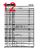
15 / 392 page  WM8281 Rev 4.0 15 RECOMMENDED OPERATING CONDITIONS PARAMETER SYMBOL MIN TYP MAX UNIT Digital supply range (Core) See notes 2, 3, 4 DCVDD 1.14 1.2 1.26 V Digital supply range (I/O) See note 5 DBVDD1, DBVDD2, DBVDD3 1.62 3.6 V LDO supply range See note 13 LDOVDD 1.71 1.8 1.89 V Charge Pump supply range CPVDD 1.71 1.8 1.89 V Speaker supply range SPKVDDL, SPKVDDR 2.4 5.5 V Analogue supply range See notes 2, 6, 7 AVDD 1.71 1.8 1.89 V Microphone Bias supply See note 8 MICVDD 0.9 2.5 3.78 V Ground See note 1 DGND, AGND, CPGND, SPKGNDL, SPKGNDR, SUBGND 0 V Power supply rise time See notes 9, 10, 11, 12 DCVDD 10 2000 µs All other supplies 10 Operating temperature range TA -40 85 °C Notes: 1. The impedance between DGND, AGND, CPGND and SUBGND should be less than 0.1 Ω.The impedance between SPKGNDL, SPKGNDR and SUBGND should be less than 0.2 Ω. 2. AVDD must be supplied before or simultaneously to DCVDD. DCVDD must not be powered if AVDD is not present. There are no other power sequencing requirements. 3. An internal LDO (powered by LDOVDD) can be used to provide the DCVDD supply. 4. ‘Sleep’ mode is supported when DCVDD is below the limits noted, provided AVDD and DBVDD1 are present. 5. If the SLIMbus interface is enabled, then the maximum DBVDD1 voltage is 1.98V. 6. The AVDD1 and AVDD2 pins should be tied together. The associated power domain is referred to as AVDD. 7. The AGND1 and AGND2 pins should be tied together. The associated ground domain is referred to as AGND. 8. An internal Charge Pump and LDO (powered by CPVDD) provide the Microphone Bias supply; the MICVDD pin should not be connected to an external supply. 9. DCVDD and MICVDD minimum rise times do not apply when these domains are powered using the internal LDOs. 10. If DCVDD is supplied externally, and the rise time exceeds 2ms, then RESET ¯¯¯¯¯¯ must be asserted (low) during the rise, and held asserted until after DCVDD is within the recommended operating limits. 11. The specified minimum power supply rise times assume a minimum decoupling capacitance of 100nF per pin. However, Cirrus Logic strongly advises that the recommended decoupling capacitors are present on the PCB and that appropriate layout guidelines are observed. 12. The specified minimum power supply rise times also assume a maximum PCB inductance of 10nH between decoupling capacitor and pin. 13. When the internal LDO is used to provide the DCVDD supply, then the LDOVDD supply must be suitably rated for the inrush current at start-up and wake-up. In the typical configuration, using the internal LDO, and with the LDOVDD / CPVDD / AVDD domains connected to a single supply, a peak current capability of 500mA is required on this supply. |
|
Link URL |
| Lei ha avuto il aiuto da alldatasheet? [ DONATE ] |
Di alldatasheet | Richest di pubblicita | contatti | Privacy Policy | Collegamento alla scheda tecnica | scambio Link | Ricerca produttore All Rights Reserved©Alldatasheet.com |
| Russian : Alldatasheetru.com | Korean : Alldatasheet.co.kr | Spanish : Alldatasheet.es | French : Alldatasheet.fr | Italian : Alldatasheetit.com Portuguese : Alldatasheetpt.com | Polish : Alldatasheet.pl | Vietnamese : Alldatasheet.vn Indian : Alldatasheet.in | Mexican : Alldatasheet.com.mx | British : Alldatasheet.co.uk | New Zealand : Alldatasheet.co.nz |
|
Family Site : ic2ic.com |
icmetro.com |
 Italian ▼
 English
 Chinese
 German
 Japanese
 Russian
 Korean
 Spanish
 French
 Italian
 Portuguese
 Polish
 Vietnamese
 Indian
 Mexican
 British
 New Zealand